
Advanced Packaging Materials Market, March 2026
- Strategic Overview: The AI Infrastructure Supercycle
The semiconductor landscape in 2026 is being fundamentally redefined by an unprecedented capital expenditure surge from US “Big Tech” titans. Google, Meta, Amazon, and Microsoft have committed to a collective investment of US 630 billion to US 720 billion—a figure that rivals the annual GDP of mid-sized nations. This “AI arms race” is the primary engine driving structural shifts in material demand and advanced packaging. We are witnessing a transition from general-purpose computing to specialized AI data center architectures, exemplified by Google’s “Ironwood” TPU and its Apollo optical circuit switch (OCS) architecture. This shift is projected to push the market share of 800G+ optical transceiver modules past 60% by the end of the year, as high-speed interconnectivity becomes the primary bottleneck for large-scale AI workloads.
Critical Constraints for the AI Data Center Buildout Procurement heads must prepare for a totalizing supply-demand imbalance that renders traditional seasonal forecasting obsolete. The pace of physical expansion is currently capped by three non-negotiable constraints:
- Electricity: Immense power draw from AI clusters is outstripping existing grid capacities, forcing a pivot toward more energy-efficient silicon photonics.
- Land: Suitable real estate with established utility infrastructure has become a premium commodity.
- Supply Chain Scalability: Structural shortages in high-end components—particularly memory and advanced substrates—are preventing the physical realization of planned compute capacity.
While infrastructure spending remains at record highs, these physical constraints have pivoted the industry’s focus toward a component-level crisis: a global memory shortage that threatens the entire electronics ecosystem.
——————————————————————————–
- The Great Memory Squeeze: Supply Constraints and Pricing Volatility
Memory has transcended its status as a commodity to become a “critical resource” in 2026. The industry is currently in a state of “panic” as capacity is aggressively reallocated toward High-Bandwidth Memory (HBM) to satisfy AI server demand. This reallocation is effectively starving traditional sectors—including smartphones, PCs, and industrial equipment—of standard DRAM and NAND. Procurement leaders must recognize that the supply gap, particularly in legacy formats like DDR4, has reached a point where Winbond executives admit it is “hard to see how it can be filled.”
2026 Memory Pricing and Supply Forecast
| Component Type | Predicted Price Movement | Capacity / Supply Status |
| DRAM (DDR4/DDR5) | Nearly 4x increase by June 2026 | Capacity fully booked through 2027 |
| SLC NAND | Projected >400% Price Jump | Extreme shortage; capacity reallocation to HBM |
| NOR Flash | 30% jump in Q1 2026 | Capacities shifted to increase MLC NAND production |
| HBM (All Gens) | Sustained high premiums | Verification bottlenecks for new market entrants |
The “Double Whammy” and Design Bottlenecks Device manufacturers are trapped in a “double whammy” scenario. On one side, Bill of Materials (BOM) costs are skyrocketing—memory now accounts for 30–40% of smartphone BOM costs, up from the historical 10–15%. On the other side, global consumer purchasing power is weakening in the smartphone and PC sectors. This is not merely a pricing issue; it is a physical design constraint. If HBM capacity remains a bottleneck, the industry must pivot toward alternative architectures to maintain performance targets without eroding margins.
——————————————————————————–
- Advanced Packaging and Materials Evolution
In the “Post-Moore era,” transistor shrinking is no longer sufficient. Advanced packaging (2.5D, 3D, and FOPLP) is now the essential bridge to meet AI’s performance and thermal requirements.
ZAM: A Strategic De-risking Move As the industry transitions from HBM3 to HBM4, Intel and SoftBank are championing Z-Angle Memory (ZAM) as a strategic “alternative” to the Samsung/SK Hynix/Micron oligopoly. Unlike HBM, which relies on complex through-silicon via (TSV) mesh routing, ZAM uses a single backbone for power and signals. For C-suite strategists, ZAM is more than a technical evolution; it is a procurement de-risking strategy designed to improve mechanical integrity for higher stacking while bypassing the current HBM supply bottleneck.
Materials Criticality and Geopolitical Intervention The physical stability of AI assemblies relies on T-Glass (Low-CTE fiberglass). Nitto Boseki currently controls 90% of this market. The strategic importance of these materials is so high that Apple has already stationed personnel in Japan at substrate suppliers like Mitsubishi Gas Chemical to secure production priority.
Advanced Packaging Capabilities and Material Requirements
| Technology | Primary Benefit | Material / Substrate Requirement |
| 2.5D / 3D Packaging | Connects logic and HBM | High-precision Silicon Interposers |
| FOPLP (Fan-Out Panel-Level) | Improved throughput / cost | T-Glass / Advanced ABF Substrates |
| Silicon Photonics | -95% Power draw vs. Trad. switches | Optical components / Low-Dk Glass |
| TGV (Through-Glass Via) | High-precision signal transmission | Glass-etched Substrates (e.g., Taesung) |
| ZAM Architecture | Backbone-based 3D stacking | Non-TSV specialized IP / 3D Assembly |
——————————————————————————–
- Competitive Landscape: Market Share and Capital Deployment
The regional realignment of the semiconductor backend is accelerating, characterized by the “Taiwan Plus One” strategy and the narrowing gap between Taiwanese and Chinese OSAT firms.
2025 Global OSAT Top 10 by Revenue (CNY Billion)
| Rank | Company | Revenue (CNY B) | Region | Strategic Context / Key Partner |
| 1 | ASE Holdings | 86.8 | Taiwan | Expanding in Penang; ADI plant acquisition |
| 2 | Amkor | 47.8 | USA | Pivoting to HDFO and AI testing |
| 3 | JCET | 40.6 | China | Tier-1 Chinese advanced packaging lead |
| 4 | Tongfu Microelectronics | 27.5 | China | Aggressive SE Asia capacity expansion |
| 5 | Tianshui Huatian | 17.3 | China | Broadening mature & advanced mix |
| 6 | Powertech | 16.7 | Taiwan | Memory-focused back-end specialist |
| 7 | WiseRoad | 16.5 | China | Scaling via global M&A and cluster growth |
| 8 | KYEC | 7.8 | Taiwan | High-end logic and AI testing focus |
| 9 | HANA Micron | 7.3 | S. Korea | Strategic Vietnam manufacturing hub |
| 10 | SJ Semi | 6.7 | China | Key back-end partner for Huawei |
The “Taiwan Plus One” Strategy To mitigate geopolitical risk, ASE is centering its overseas manufacturing in Penang, Malaysia. This shift is solidified by the acquisition of Analog Devices’ (ADI) Penang facility, expected to close in 2Q26. This allows ASE to package non-Taiwan-produced wafers in a high-tech, automated hub, reducing exposure to cross-strait tensions.
2026 PCB/Substrate Capital Expenditure Benchmark
| Manufacturer | 2026 Planned CapEx (USD) | Primary Strategic Focus |
| Zhen Ding | $1.6 Billion | 10 plants under construction (Thailand, Kaohsiung) |
| Kinsus | $960 Million | High-end ABF substrate capacity expansion |
| Unimicron | $810 Million | Advanced ABF lines for next-gen AI platforms |
| Kingboard | $540 Million | High-end multilayer boards (Thailand/Taiwan) |
——————————————————————————–
- Process Reliability, Testing, and Quality Assurance
As we move toward multi-die “chiplet” assemblies, the complexity of inspection has tripled. In the high-value AI sector, “Zero Defect” is a non-negotiable requirement.
Testing Methodologies and Reliability Risks Traditional optical inspection (AOI) is no longer sufficient to detect subsurface failures. The primary site of breakage in 2.5D/3D assemblies is now the thinned silicon interposer, which is susceptible to crystalline defects during backside grinding and thermal compression.
- Subsurface Cracks: Requires X-ray Topography (XRT) to select Known Good Die (KGD) prior to bonding.
- Bond Integrity: Acoustic Microscopy (SAM) is essential for detecting delamination and voids in thinned stacks.
- Head-in-Pillow (HiP): Hidden bond failures require high-resolution X-ray inspection to prevent field escapes.
- High-Power Burn-in: Aehr Test Systems has seen a valuation surge following purchase orders for “ultra-high-power” AI processor testing, essential for data center reliability.
——————————————————————————–
- Outlook: 2026-2027 Market Trajectory
As we look toward 2027, the market is defined by a sharp divergence between AI-driven growth and consumer-sector stagnation.
- Growth Engines: AI servers, Wi-Fi 7, and LEO satellite hardware (LEO antenna modules) are offsetting decade-low slumps in traditional home appliances and mid-range smartphones. Foxconn expects its AI server market share to exceed 40% as its Component Module Move (CMM) strategy scales.
- The 9-Month Window: While the memory supply crunch may see relief in approximately nine months, this window is precarious. China’s export controls on tungsten carbide—essential for the production of PCB drills—have already caused a 15% price spike in white drills. This, combined with volatility in precious metals, could create a secondary bottleneck cycle just as the memory crisis begins to ease.
The semiconductor packaging market of 2026 remains a high-stakes environment where technical leadership in 3D integration must be matched by aggressive material procurement strategies to survive the AI supercycle.
The 2026 Semiconductor Materials Paradox: High-Margin Scarcity and the AI Supercycle
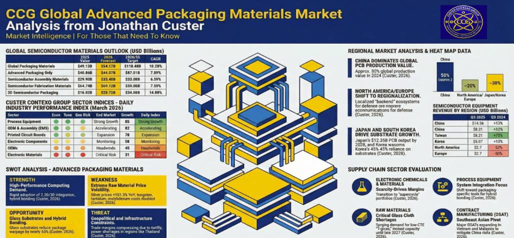
The global semiconductor industry has reached a watershed moment in 2026, navigating a complex paradox where soaring demand for artificial intelligence infrastructure has pushed industry revenues toward the US 1 trillion mark while simultaneously destabilizing downstream supply chains for consumer electronics .[1] Total annual sales for these cto rare projected to hit US 975 billion this year, reflecting a staggering 26% growth rate following a robust 22% expansion in 2025.[1] This acceleration is not uniform; rather, it is driven by a stark structural divergence where approximately 50% of industry revenue is now generated by generative AI chips, despite these components representing less than 0.2% of total unit volume.[1]
For a global materials leader like Henkel, this shift from a high-volume, low-margin paradigm to a high-margin, low-volume “supercycle” necessitates a fundamental reconfiguration of the materials portfolio.[1] The relentless pursuit of computing power has accelerated the adoption of advanced packaging platforms, including 2.5D interposers, 3D-stacked memory (HBM), and chiplet-based architectures.[2, 3] These technologies are no longer secondary considerations but the primary enablers of system-level performance gains, particularly as traditional front-end lithography scaling reaches the physical limits of Moore’s Law.[2, 4]
The industry mandate for 2026 is the management of systemic risks, primarily centered on critical component shortages and the massive capital intensity of advanced backend facilities.[1, 5] Supply chain CEOs must now balance the “zero-sum” competition for wafer and packaging capacity, particularly as hyperscale data center buildouts threaten to consume 70% of high-end memory supply.[6] This research report provides a comprehensive intelligence summary of the current materials landscape, process requirements, and competitive positioning as of early 2026.
Market Valuation and Forecast Metrics
The global semiconductor packaging materials market is valued at USD 54.17 billion in 2026, maintaining a trajectory to reach USD 118.48 billion by 2034 with a 10.28% Compound Annual Growth Rate (CAGR).[7] This growth is primarily catalyzed by the expansion of the advanced packaging segment, which is expected to outpace traditional formats significantly.[8, 9]
| Market Segment | 2025 Value (USD) | 2026 Forecast (USD) | 2034/35 Target (USD) | CAGR |
| Global IC Packaging Materials | 49.12 Billion | 54.17 Billion | 118.48 Billion | 10.28% [7] |
| Advanced Semiconductor Packaging | 41.55 Billion | 44.90 Billion | 83.35 Billion | 8.04% [10] |
| 3D Semiconductor Packaging | 18.02 Billion | 20.75 Billion | 36.06 Billion | 14.80% [11] |
| Heterogeneous Integration Tech | 16.20 Billion | 18.40 Billion* | 50.60 Billion | 13.50% [12] |
| Semiconductor Underfill Materials | 197.6 Million | 215.2 Million | 463.6 Million | 8.90% [13] |
| Silver Sintering Paste | 545.0 Million | 598.0 Million* | 1,379.65 Million | 9.74% [14] |
*Calculated based on 2025 base and stated CAGR.
Geopolitically, the Asia-Pacific region maintains its dominance, accounting for roughly 46-54% of the global market.[7, 15] However, a significant realignment is underway as North America and Europe incentivize the development of domestic “backend” ecosystems.[16] The United States, through the CHIPS and Science Act, has issued billions in grants and loan guarantees, prompting major players like Amkor and SK Hynix to establish advanced packaging facilities in Arizona and Indiana, respectively.[6, 16]
Electronic Materials: Technical Evolution and Requirements
Die Attach Paste (DAP) and Film (DAF)
Die attach technology in 2026 is moving away from purely mechanical fixation toward a multifunctional role encompassing thermal dissipation and electrical connectivity in high-stress environments.[17, 18] Die attach film (DAF) has seen robust growth, valued at USD 1.33 billion in 2026, as it facilitates the ultra-thin profiles required for multi-die memory stacks in smartphones and high-performance laptops.[19]
The primary technical driver for DAF is the reduction of thickness down to single-digit micrometers, enabling the vertical stacking of 16 to 24 dies without compromising the Z-height of the final package.[20, 21] Conversely, liquid die attach paste (DAP) remains the standard for large-body application-specific integrated circuits (ASICs) and power modules where void-free coverage and thickness uniformity are difficult to achieve with films.[18, 22]
Market segmentation for die attach materials reveals a strong preference for epoxy-based adhesives in consumer electronics due to their favorable moisture resistance and balance of performance and cost.[23, 24] However, high-power segments are aggressively adopting silver sintering and eutectic attach methods to meet the thermal demands of next-generation SiC and GaN devices.[24, 25]
The Sintering Transition: Silver vs. Copper
Sintering has emerged as the definitive interconnect technology for the automotive power electronics sector in 2026.[26, 27] The transition from conventional solder to silver sintering is driven by the specific operational requirements of Silicon Carbide (SiC) MOSFETs, which frequently operate at junction temperatures exceeding 175°C.[25, 27] Under these conditions, traditional SAC (Tin-Silver-Copper) solders demonstrate failure rates above 8% due to thermal fatigue and creep.[27]
| Interconnect Type | Thermal Conductivity (W/m·K) | Max Operating Temp (°C) | Mechanical Strength (MPa) |
| SAC Solder | < 65 | < 150 | ~ 10-15 [28] |
| Silver Sintering Paste | > 200 | > 300 | > 25 [27] |
| Copper Sintering Paste | > 250 | > 350 | > 30 [29] |
Silver sintering paste currently holds the majority share of the sintered interconnect market, with nano-silver formulations dominating the segment (47% share in 2025) because they enable lower sintering temperatures and superior bonding strength.[14, 30] However, the spike in silver prices in late 2025 has created an opening for copper sintering, which is expected to expand at a CAGR of 40.2% through 2033.[26, 29]
Copper sintering offers higher thermal conductivity and a closer CTE match to silicon, but it faces technical hurdles related to oxidation during the sintering process.[29, 31] In 2026, leading manufacturers like Heraeus and Indium are increasingly offering “hybrid” pastes that combine nano and micron-sized particles to optimize performance while reducing raw material costs.[14, 29]
Underfill Materials: CUF, LMUF, and LMC
Underfill materials have become essential for ensuring the structural integrity of flip-chip and 2.5D packages as interconnect pitches shrink below 80 µm.[13, 16] Capillary Underfill (CUF) maintains a 40% market share, favored for its ability to flow into narrow gaps through surface tension.[13]
A significant trend in 2026 is the adoption of Molded Underfill (MUF) and Liquid Molded Underfill (LMUF), which allow for the simultaneous encapsulation and underfilling of high-density chips.[32, 33] This technique is particularly valuable in high-volume smartphone production where it can reduce chip failure rates by 50% and improve drop resistance by 25%.[32] LMUF, in particular, is witnessing a 6.39% CAGR as manufacturers prioritize low-viscosity formulations that can handle the high-throughput requirements of 5G and AI hardware.[33, 34]
Liquid Molding Compounds (LMC) are also gaining ground in the power module sector, providing robust protection for SiC and GaN devices in harsh automotive environments.[35, 36] Henkel’s latest polyurethane and epoxy-based potting compounds, such as the Loctite STYCAST series, have been engineered with ultra-low ionic content (<20 ppm) to minimize corrosion and prevent silver migration in high-humidity conditions.[35]
Thermal Interface Materials (TIM): The Heat Dissipation Frontier
Thermal management is widely recognized by industry analysts as the primary limiting factor for 3D heterogeneous integration in 2026.[37, 38] AI servers generating hundreds of watts per package require TIMs with exceptionally low thermal resistance and high reliability over thousands of power cycles.[39, 40]
Indium-based metal TIMs and InAg alloys are replacing traditional thermal greases in high-performance applications due to their ability to provide superior contact area even under microscopic surface roughness.[39, 40] Investigations indicate that while air-cooled 2.5D stacks are feasible up to 300 W, any configuration exceeding 350 W necessitates liquid or hybrid cooling in conjunction with high-performance TIMs.[38] The global TIM market is projected to exceed US$7 billion by 2036, growing at a CAGR of 10% from its 2026 baseline.[41]
Semiconductor Packaging Architectures
High Bandwidth Memory (HBM) and the Transition to HBM4
The HBM market is currently in a state of hyper-growth, with memory semiconductors emerging as the primary driver of both industry demand and profitability.[42, 43] Major analysts expect HBM3E to remain the flagship product in 2026, accounting for approximately two-thirds of total shipments.[42, 44] However, the race for HBM4 has already reached an inflection point, with major suppliers like SK Hynix and Samsung delivering paid samples to NVIDIA in the first quarter of 2026.[44]
| HBM Generation | Max Bandwidth | Layer Count | 2026 Status |
| HBM3 | 3.35 TB/s | 8-12 | Standard in H100 AI Accelerators.[43] |
| HBM3E | 4.8 TB/s | 12 | Dominant in B200 / Blackwell platform.[42, 43] |
| HBM4 | > 2.0 TB/s* | 16 | Sampling 1Q 2026; mass production 3Q 2026.[21] |
*Note: Bandwidth per stack doubles the channels of HBM3E.
The transition to HBM4 involves a “massive architectural overhaul,” shifting from traditional microbumps to Cu-Cu hybrid bonding to reduce latency and power consumption.[21, 43] This change places immense pressure on the material supply chain for through-silicon vias (TSVs) and advanced interposer substrates.[45, 46]
2.5D and 3D Packaging: CoWoS and Beyond
2.5D packaging, characterized by placing dies side-by-side on a shared interposer, has become the de facto standard for AI training clusters.[16, 47] TSMC’s CoWoS capacity remained severely constrained throughout 2025, with utilization rates above 95%, forcing customers like NVIDIA and AMD to secure production slots through 2027.[16, 48]
The primary bottleneck in 2.5D production is the supply of Ajinomoto Build-up Film (ABF) substrates.[16] Capacity expansions at major suppliers like Ibiden and Shinko Electric are not expected to reach full volume until mid-2026, leaving lead times for high-layer-count substrates at roughly 38 weeks.[16] This shortage has accelerated the search for alternative substrate materials, including glass cores, which offer superior dimensional stability and enhanced high-speed I/O performance.[49, 50] Glass substrate shipments are projected to grow at a CAGR of 33% in the HBM and logic segments as they begin to replace organic substrates in high-end HPC markets by 2030.[50]
Power Modules and the 800-Volt Influence
The electrification of global transportation is driving a surge in demand for power modules that can survive the harsh environment of an EV drivetrain.[26, 51] Modern 800-volt vehicle architectures require semiconductors that can withstand repeated thermal cycles of 150°C and maintain stability at junction temperatures above 200°C.[16, 51]
Silicon Carbide (SiC) MOSFETs have captured over 60% of the automotive power segment by late 2025.[51, 52] The packaging of these devices has shifted from traditional wire bonding to copper clips and die-top systems, utilizing silver or copper sintering for the primary die-attach layer.[26, 28] This structural shift has created a massive market for ceramic packaging materials like aluminum nitride (AlN), which are valued for their durability and heat resistance in high-voltage power management systems.[53, 54]
Process Science and Failure Mechanisms
Bondline Thickness (BLT) and Warpage Control
As package complexity increases, the management of Bondline Thickness (BLT) has become a critical predictor of device reliability.[55] Coupled thermal-mechanical simulations of large-body high-density fan-out (HDFO) packages show that BLT variation is a major contributor to inconsistent temperature fields across the die.[55] In typical AI server ASICs, a thinner bond line at the center of the die compared to the corners can create a temperature delta of 9.7°C, increasing the risk of localized hotspots and thermal-induced cracking.[55]
Warpage is the secondary primary cause of yield loss in 3D structures, driven by the CTE mismatch between dissimilar materials such as silicon, metal, and encapsulation resins.[37, 56] Strategies to mitigate warpage include lowering reflow and resin curing temperatures, ensuring structural symmetry in the package design, and utilizing low-modulus materials to relieve internal stresses.[37]
Delamination, Voids, and Cracks
Delamination between the die, underfill, and molding compound is the most frequent failure mode observed in Temperature Cycling Tests (TCT).[57] The repeated expansion and contraction of these layers can lead to the accumulation of residual stresses, eventually weakening the adhesion interfaces.[57]
Voiding within the sintered silver or solder layer is another significant concern. Research in 2025 indicated that even small voids in the die-attach layer can become thermal barriers, leading to a 25% increase in junction temperature and potential device failure under high current pulses.[58, 59] Optimizing the drying temperature and heating rate in sintering processes has been shown to reduce porosity to 2-3%, ensuring a structurally uniform and dense joint.[60]
Metrology and Inspection Systems
The increasing structural complexity of stacked layers has necessitated the development of advanced MET (Metrology, Inspection, and Testing) systems.[61] Detection of “buried” defects and voids now requires hybrid inspection platforms that combine optical, X-ray, and electron-beam technologies.[61]
Market-leading metrology firms like Onto Innovation reported that orders from 2.5D packaging for AI devices more than doubled in the final quarter of 2025.[48, 62] The use of AI and Machine Learning (ML) in inspection is also revolutionary, enabling real-time defect classification and predictive failure analysis, which reduces false positives and optimizes final yields in expensive multi-die stacks.[61, 63]
Reliability Testing and 2026 Global Standards
The electronics industry is operating under five pivotal new standards published in early 2026, redefining benchmarks for solderability and component durability.[64]
New IEC Standards for 2026
- EN IEC 60749-21:2026: This standard provides updated “dip and look” test methods for both through-hole and surface-mount devices, aligning test conditions with contemporary lead-free manufacturing environments.[64]
- EN IEC 60749-22-2:2026: Focused on wire bond shear testing, this revision expands coverage to include copper and silver alloy wires, requiring precise measurement of bond diameters and shear test placement.[65]
- EN IEC 60749-7:2026: This definitive standard for testing moisture and atmospheric gas composition within hermetically sealed devices now utilizes advanced mass spectrometry to validate seal quality in mission-critical applications.[65]
Critical Reliability Protocols
Manufacturers in 2026 are increasingly moving beyond standard qualifications toward lifetime modeling tailored to specific environmental stressors.[66, 67]
| Reliability Test | Parameter / Standard | 2026 Industry Significance |
| TCT (Temp Cycling) | 1,000 cycles; -65 to +150°C | Measures ability to withstand material fatigue.[57] |
| HAST (Highly Accel.) | JESD22-A110; 85/85 test | Simulates humid environments; accelerates moisture penetration.[57] |
| Power Cycling (PC) | PCsec (<5s); PCmin (>15s) | PCmin is crucial for SiC; targets solder joint and baseplate fatigue.[67] |
| MSL (Moisture Sens.) | JEDEC J-STD-020 | Baseline for floor-life; MSL1 is the goal for automotive zero-delamination.[66, 68] |
| ESD HBM | JS-001-2017; 2,000 V | Validates protection against electrostatic discharge.[69] |
Wolfspeed’s reliability data for 200mm SiC wafers indicates that improved crystal growth has significantly reduced micropipe densities and threading screw dislocations, directly improving the long-term wear-out profiles of power modules.[66]
Competitive Market Analysis: 2026 Landscape
The semiconductor packaging materials market in 2026 is highly concentrated, with a few established global players controlling the majority of the supply for high-end applications.[70]
Henkel: Strategic Positioning and Portfolio
Henkel Adhesive Technologies remains the undisputed global market leader in the 60 billion euro adhesives industry, holding an estimated 22% share.[71] Within the molded underfill segment, Henkel also holds a 22% global share, leveraging its strong presence in both consumer and industrial electronics.[32] Henkel’s 2026 strategy focuses on high-growth industrial adjacencies, specifically e-mobility and advanced medical devices.[71, 72]
A significant competitive advantage for Henkel is its “sustainability-first” R&D engine. The company has responded to silver price volatility by introducing silver-plated copper (SPC) ink technology, which offers lower price volatility while maintaining technical performance for printed electronics.[72] Henkel’s ambitious sustainability goal is to achieve net-zero greenhouse gas emissions by 2045, a commitment that aligns with the increasing demand from OEMs for “green” manufacturing materials.[73, 74]
Resonac: The EMC and Back-End Specialist
Resonac Holdings (formerly Showa Denko Materials) is the global leader in semiconductor epoxy molding compounds (EMC), commanding roughly 40-50% of the market in 2025.[75] Resonac has positioned itself as the primary materials partner for the HBM and AI server ecosystem.[75, 76] The company has invested heavily in “AI-related materials,” including copper-clad laminates (CCL) and specialized TIMs.[77]
Resonac’s proprietary “Neural Network Potential” (NNP) technology allows for the discovery of new materials by simulating chemical reactions 10 times faster than traditional methods, providing a decisive edge in the race for HBM4-compatible formulations.[78]
Kyocera: Fine Ceramics and Hermetic Packaging
Kyocera Corporation utilizes its heritage in fine ceramics to dominate the ceramic packaging segment, which is forecast to grow at an 11.67% CAGR through 2031.[16, 78] Kyocera’s expansion of its Kokubu Plant in late 2024 has allowed it to meet the surge in demand for AlN ceramic components used in 800V EV inverters and semiconductor manufacturing equipment.[16, 78]
Sumitomo Bakelite: The High-Reliability Competitor
Sumitomo Bakelite remains a primary rival to Resonac in the EMC market, competing on price-performance and long-term reliability for automotive-grade ICs.[75] Sumitomo is also a leading provider of die attach films (DAF), positioning it as a critical supplier for both traditional and advanced stack packaging.[19, 79]
Specialist Players: Alpha, Heraeus, and Tanaka
- Heraeus Electronics: The largest manufacturer in the full-silver sintering paste market, holding over 32% revenue share in 2024.[80, 81] Heraeus has aggressively expanded its portfolio to support wide-bandgap applications in EVs and renewable energy.[14, 82]
- Alpha Assembly Solutions (MacDermid Alpha): Holds approximately 15% of the silver sintering market share.[81, 83] Alpha recently introduced enhanced sintering formulations designed to improve thermal cycling reliability in complex power modules.[14]
- Tanaka Precious Metals: A global leader in bonding wires and precious-metal-based materials. Tanaka has seen a surge in inquiries from the Indian market following the launch of the India Semiconductor Mission and is currently conducting due diligence for a local manufacturing facility.[84]
- Namics Corporation: A high-end specialist in underfill materials and low-viscosity formulations for 5G modems and RF modules.[13, 33] Namics is a key competitor to Henkel in the flip-chip and CSP segments.[13, 85]
Emerging Chinese Entrants: Yizbond, Yongoo, and Bonotec
The domestic Chinese materials market is expanding rapidly, with local suppliers increasing their market share by 9% annually since 2020.[86]
- Yizbond and Yongoo: These firms are scaling production of epoxy-based adhesives and die attach pastes, primarily targeting the cost-sensitive consumer electronics and mobile device segments.[17, 87]
- Bonotec: Gaining traction by offering specialized conductive adhesives and packaging chemistries that provide a localized alternative to international suppliers within the Chinese fab ecosystem.[75, 86]
Chinese firms are benefiting from significant government support through the “Made in China 2025” initiative, which aims to transform the country into a global leader in advanced semiconductor technologies.[9]
Geopolitical Shifts and Supply Chain Resilience
In 2026, geopolitics has emerged as a primary market driver, often rivaling demand in its impact on costs and sourcing strategies.[1, 88] The supply chain is caught in a moment of contradiction: while global inventory levels have largely stabilized, the sense of security is misleading.[89, 90]
One of the most disruptive narratives entering 2026 is the tension within Nexperia, which was split into Dutch and Chinese entities in late 2025.[89] China’s response—imposing export controls on components originated by Nexperia—sent ripples through the automotive sector, pushing lead times out by six to eight weeks.[89] Many automakers have responded by returning to “COVID-era planning,” stretching component inventories and slowing production schedules to avoid line stoppages.[89]
Furthermore, new United States tariffs implemented in 2025 have driven combined effective rates on certain Asian substrate components as high as 25%.[91, 92] This has compelled OEMs to diversify their qualified suppliers and regionalize manufacturing to maintain operational continuity.[1, 93]
The Convergence of Sustainability and Digital R&D
A transformative trend in 2026 is the integration of circular economy principles into the materials value chain.[93, 94] Compliance with new regulatory frameworks, such as the EU Digital Product Passports and Extended Producer Responsibility (EPR), is being converted from a cost burden into a strategic source of competitive advantage.[94]
Green Material Trends
- Recycled Silver: High silver prices have accelerated the use of recycled silver as a raw material in conductive inks and sintering pastes.[72]
- Halogen-Free and Low-VOC:
Click Below for Presentation: